E-mail
WhatsApp


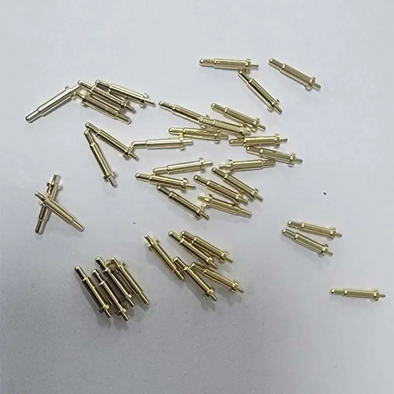
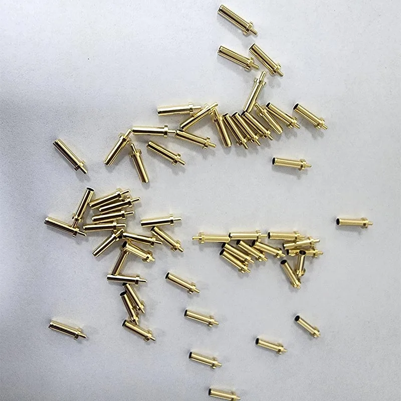
Qiyiguo Technology has long specialized in the R&D and precision manufacturing of Pogo Pins. Leveraging a dual quality control system and end-to-end precision machining processes, its circuit board test probes cover applications ranging from standard pitches to ultra-fine pitches (as low as 0.2mm). Our company provides a comprehensive range of test probes, including both standardized models and custom-engineered solutions, to industries such as PCB fixture manufacturing, electronics contract manufacturing, and semiconductor testing.
1. Application Positioning: Standard pogo pins are used for permanent electrical connections within electronic devices; circuit board test probes are designed specifically for mass-production PCB testing, chip verification, and burn-in screening, serving as temporary, precision electrical interfaces for quality assurance processes.
2. Precision and Consistency: Standard pogo pins require only batch-level parameter uniformity; test probes demand high consistency in spring force, contact resistance, and stroke across individual units to ensure data integrity in massive pin-array tests and eliminate batch testing errors.
3. Structural Adaptability: Standard pogo pins feature limited tip designs for fixed applications; test probes offer a wide variety of specialized tip structures tailored to specific test points, such as bare copper pads, SMD solder joints, vias, BGA solder balls, and component leads.
4. Electrical Performance: Standard pogo pins typically meet requirements with contact resistance ≤30mΩ; test probes utilize precision gold-plating processes to achieve resistance as low as <10mΩ, preventing false test results caused by minor resistance deviations and ensuring measurement accuracy.
5. Density Adaptability: Standard pogo pins are designed for conventional spacing; test probes support ultra-fine pitch arrangements (down to 0.2mm), perfectly meeting the testing needs of high-density precision PCBs and miniature chip packages.
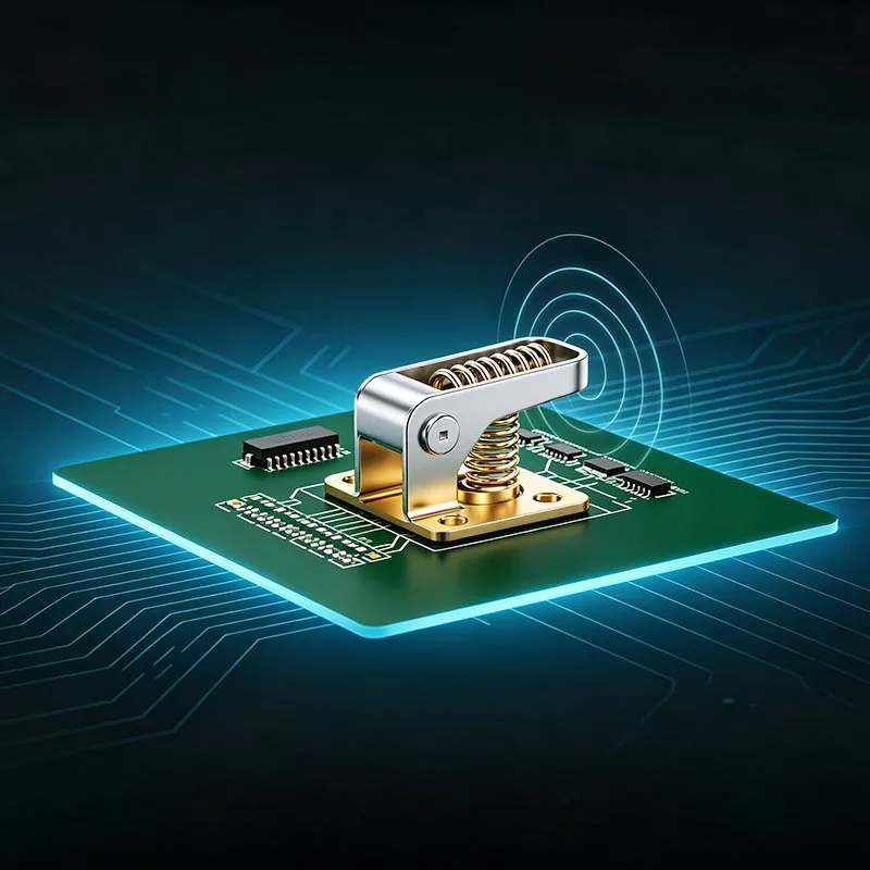
In their natural state, the probe tips extend from the barrel; during testing, downward pressure causes the tip to retract and compress the internal spring, maintaining firm contact with the test pad through constant pressure. During the compression and contact process, slight friction from the tip automatically removes surface oxidation and dust/impurities from the pad, further reducing contact resistance. When multiple probes are integrated into a test fixture (bed-of-nails), they enable simultaneous multi-point conduction, allowing for automated, batch electrical parameter testing of the entire PCB.
Parameters cover a full range of scenarios, including ultra-fine pitch, micro-resistance, high current, high frequency, and wide temperature ranges, meeting testing standards for consumer electronics, industrial applications, semiconductors, and automotive PCBs.
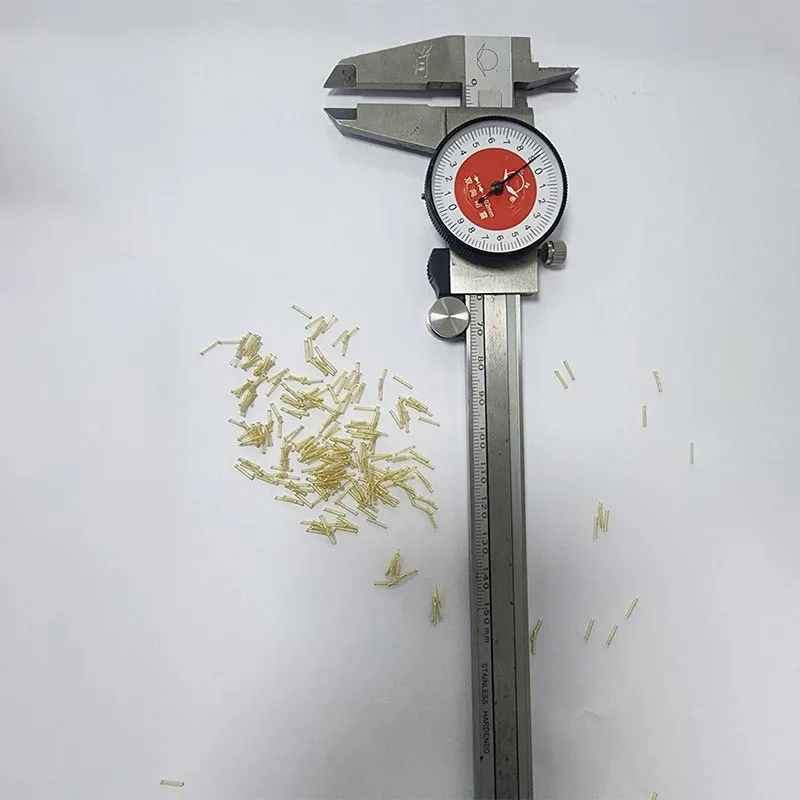
- Probe Barrel Diameter & Pitch: 0.3mm–3.0mm; ultra-fine pitch capability supports 0.2mm high-density testing.
- Overall Dimensions: Total length 5.0mm–70.0mm; working stroke 0.3mm–5.0mm; adaptable to various fixture assembly heights.
- Contact Force: Customizable range of 50g–500g; meets diverse needs ranging from preventing damage to thin boards to ensuring stable contact with thick boards.
- Electrical Precision: Standard contact resistance ≤30mΩ; high-precision gold-plated models ≤10mΩ; minimal measurement error.
- Load-bearing Performance: Rated current 0.5A–10A; high-current custom models exceed 35A; maximum withstand voltage of 500V.
- Mechanical Lifespan: Standard models ≥10,000 compression cycles; high-end precision models exceed 100,000 cycles.
- Operating Temperature: -40°C to +150°C; suitable for high/low-temperature burn-in testing conditions.
- High-Frequency Performance: RF probes feature a -1dB bandwidth up to 27.9GHz, enabling precise high-frequency signal testing.
- Environmental Compliance: Fully compliant with RoHS 2.0 and REACH standards; suitable for global mass production and export.
Leveraging ISO9001 and IATF16949 dual-certification systems and implementing the five core automotive quality tools, we ensure full-process control and traceability, from design and manufacturing to the finished product, meeting entry standards for high-end electronics manufacturing and automotive supply chains.
Comprehensive implementation of APQP (Advanced Product Quality Planning), PPAP (Production Part Approval Process), FMEA (Failure Mode and Effects Analysis), SPC (Statistical Process Control), and MSA (Measurement System Analysis). These measures proactively mitigate common failure issues such as force degradation, resistance drift, tip wear, and barrel deformation, achieving a process capability (Cpk) of ≥1.33 for critical processes.
Equipped with a full range of testing instruments, including CMMs, optical projectors, contact resistance testers, spring force testers, X-ray coating thickness gauges, salt spray chambers, lifespan testers, and high-frequency network analyzers, we conduct comprehensive verification across dimensional, electrical, mechanical, environmental, and high-frequency performance parameters.
For every product batch, we retain raw material reports, process records, and finished product inspection reports. This ensures full-process traceability, meeting the quality traceability requirements of high-end clients regarding factory audits, certifications, and mass production.
You provide PCB test point layouts, fixture parameters, and electrical performance requirements; our engineering team completes a dedicated DFM review within 48 hours. We precisely match head styles, spring force, travel, plating, and tail structures to deliver the optimal testing solution.
Standard models are available for rapid delivery, while custom models are prototyped within 5–7 working days. We support everything from small-batch pilot runs to stable mass production, with flexible minimum order quantities (MOQs).
We support various packaging methods, including bulk, tube, and tape-and-reel, to suit automated assembly needs. Services such as VMI (Vendor Managed Inventory) and JIT (Just-In-Time) delivery are available to align with the client's lean manufacturing schedules.
PCB testing requires the precise capture of minute deviations in electrical parameters. Standard spring pins often exhibit high resistance and poor stability, leading to issues such as false readings, misjudgments, and parameter drift. Specialized Circuit Board Test Probes undergo precision gold-plating processes; their resistance is stably controlled within 10mΩ, ensuring high contact consistency. This minimizes testing errors and guarantees accuracy in high-volume yield testing.
0.2mm ultra-fine pitch probes are designed for high-density precision PCBs, miniature BGA chips, and precision circuits in wearable devices, addressing issues such as excessive pitch, point-to-point interference, and alignment difficulties found in conventional probes. Through micron-level grinding and coaxiality control, these probes eliminate short circuits between adjacent points and alignment errors, making them suitable for mass production testing of high-end precision circuit boards.
Spear-point tips are suitable for oxidized bare copper pads, as they can pierce the surface oxide layer; flat tips suit flat SMD solder terminals, ensuring uniform contact pressure; spherical tips are ideal for via continuity testing, offering precise automatic centering; claw/hook tips are used for testing through-hole component leads; and spade-shaped tips accommodate irregularly shaped or narrow-edge pads, selecting the right tip significantly enhances testing stability.
High-current probes feature enlarged conductive barrels and contact surfaces to optimize current transmission paths, thereby reducing heat generation and voltage drop under high-current conditions. Capable of carrying currents exceeding 35A, they are specifically designed for power network and high-power module testing on PCBs; conventional probes are prone to overheating and unstable conductivity under high-current loads and cannot be used as substitutes.
Specialized RF probes utilize high-end rhodium plating and impedance-matching structures to minimize parasitic parameters and reduce high-frequency loss. With a bandwidth exceeding 27.9 GHz, they accurately capture high-frequency signal parameters without attenuation or distortion, fully meeting the high-frequency testing requirements of communication PCBs and RF modules.