E-mail
WhatsApp



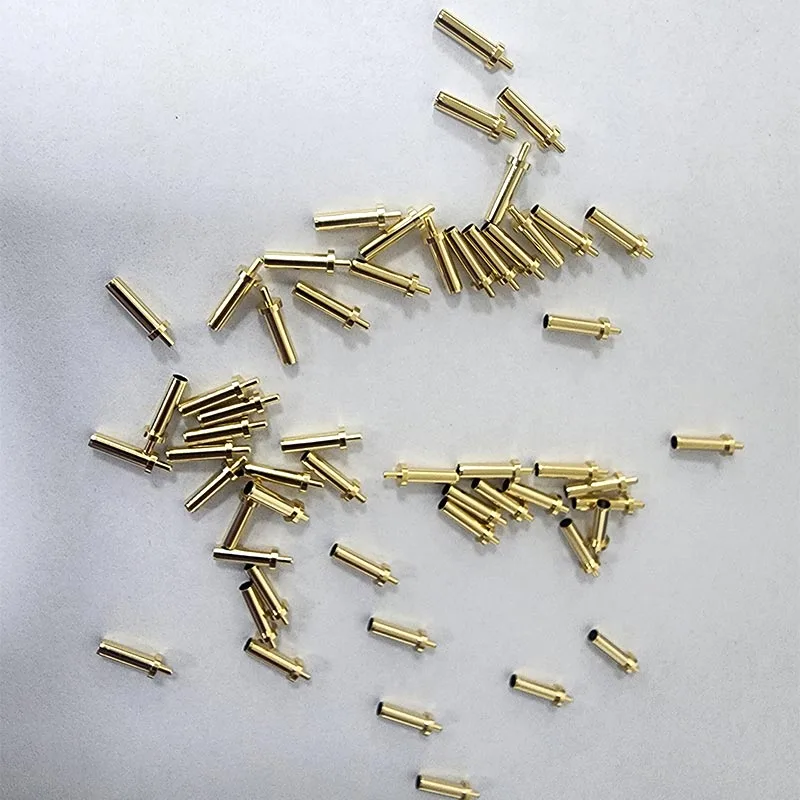
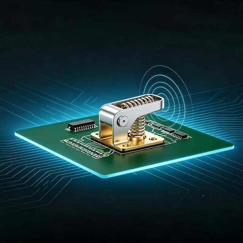
PCB Test Probe Pogo Pins are indispensable precision consumables in the electronics manufacturing and testing process. Acting as a bridge between testing equipment and PCB test points, they facilitate electrical continuity through precise, spring-loaded contact, enabling comprehensive electrical testing across stages ranging from bare boards to assembled units and final functional verification.
Whether it involves simultaneous contact with thousands of test points during In-Circuit Testing (ICT), micron-level precision positioning in flying probe testing, or chip-level testing for BGA packages, the performance of the test probe directly determines test reliability and production efficiency.


The core functions of a PCB Test Probe Pogo Pin include electrical connection, pressure buffering, and precise positioning.
Its structure consists of four main parts:
Tip/Plunger: The front contact element responsible for making contact and penetrating oxidation layers. Tips come in various shapes (pointed/spear, flat, round/spherical, spade, claw/hook, etc.) and feature gold plating to ensure low contact resistance.
Spring: Located inside the barrel, it provides continuous, stable axial force to the tip, ensuring reliable contact under varying conditions of vibration and manufacturing tolerances.
Barrel/Tube: A hollow cylinder that houses the tip and spring, serving as both the current conduction path and the mechanical structural support.
Tail: The rear connection point, which interfaces with the test fixture or testing equipment via methods such as a solder tail or banana plug.
In its initial state, the tip extends slightly beyond the barrel due to the spring's action. When the probe contacts a PCB test point, the tip retracts under pressure, compressing the internal spring. The constant spring force (typically 100g–200g) ensures a reliable, low-resistance electrical connection between the tip and the test point.
During the repeated extension and retraction of the probe, the slight friction between the probe tip and the test point helps remove minor oxide layers or contaminants from the contact surface, thereby enhancing contact reliability.
In mass testing, a large number of test probes are integrated into a "Bed-of-Nails" fixture; precise positioning allows the probe array to simultaneously and accurately contact multiple test points on the PCB, enabling efficient automated testing.
| Comparison Dimension | Regular Connecting Spring Pins | PCB Test Probes |
| Core Application | Permanent electrical connections inside finished products | Temporary electrical contact during testing procedures |
| Life Requirement | Tens of thousands to hundreds of thousands of cycles | Thousands to tens of thousands of cycles (precision consumable parts) |
| Contact Resistance | ≤30 mΩ is acceptable | Lower and more stable resistance required, directly affecting measurement accuracy |
| Pin Tip Type | Relatively fixed styles | Highly diversified tips for different test points (sharp tip, flat tip, claw tip, etc.) |
| Rear-end Connection | Soldered or press-fitted onto PCB | Solder shank or banana plug for test fixture mating |
| Density Requirement | Standard pitch spacing | High-density fine pitch, pitch down to 0.2 mm |
| Consistency Requirement | Consistent performance across batches | Strict consistency for spring force and resistance on every single probe |
● ICT (In-Circuit Test) Probes: Used in ICT fixtures to contact thousands of test points simultaneously, measuring the electrical parameters of individual components (resistance, capacitance, inductance, diode polarity, etc.).
● Flying Probe Test Probes: Used in flying probe equipment, where 4–8 independently driven, fine probes move at high speed along the X, Y, and Z axes to contact test pads point-by-point.
● FCT (Functional Test) Probes: Used in functional test fixtures to simulate real-world operating conditions and verify the functionality of the entire board.
● BGA Test Probes: Specifically designed for BGA (Ball Grid Array) package and chip testing, accommodating fine solder ball pitches.
● Programming/Burn-in Test Probes: Used for chip programming and high-temperature burn-in reliability testing.
● Spear Point: High penetrating power; capable of piercing oxide layers; suitable for testing bare copper pads.
● Flat Point: Large contact area with uniform pressure distribution; suitable for flat pads and SMD terminations.
● Crown/Ball Point: Good self-centering capability; suitable for testing via holes.
● Scoop Point: Suitable for test pads with specific shapes.
● Claw/Hook Point: Capable of hooking onto component leads or the edges of solder pads; suitable for testing through-hole component leads.
● Solder-tail type: The tail is a solderable cylindrical post soldered directly onto the test fixture PCB.
● Banana plug type: The tail is a banana plug that inserts directly into the test equipment's socket.
● Crimp type: The tail connects to a wire via crimping.
● RF probe: Designed for high-frequency signal testing; features excellent impedance matching and low parasitic parameters.
● High-current probe: Suitable for power network testing; capable of handling high current loads.
● Kelvin probe: Uses a four-wire measurement method to eliminate lead resistance effects; suitable for high-precision resistance measurement.
● Switch probe: Features an integrated switch function for testing circuit continuity (on/off control).
● Pneumatic probe: Uses pneumatic actuation for probe extension and retraction; suitable for automated test production lines.
● ICT (In-Circuit Test): Testing after PCB assembly—probe arrays contact thousands of test points simultaneously to precisely verify the solder quality and electrical parameters of each component.
● Flying probe test: Electrical testing of bare boards before shipment—no custom fixture required; 4–8 probes move at high speed to test point-by-point; suitable for small-batch, high-mix production.
● BGA/Chip testing: Semiconductor package testing—fine-pitch probe arrays make precise contact with BGA solder balls to perform chip-level electrical parameter testing.
● Programming and burn-in testing: Reliability verification before mass production continuous testing under extreme conditions (e.g., high temperature, high humidity) to screen out defective units.
● Boundary scan testing: Pin connection testing for high-density PCBs—detects open circuits and short circuits on bottom-side pins (such as BGAs) via the JTAG interface.
● Functional Test (FCT): Functional verification after powering up the board—probes provide power and signal interfaces to simulate real-world operating conditions.
● PCB repair and debugging: Manual testing by engineers—handheld spring-loaded probes quickly contact test points for signal measurement using an oscilloscope or multimeter.
| Component | Common Materials | Process Features |
| Pin Tip | Beryllium Copper (BeCu), High-carbon Steel, Brass C3604, Nickel Silver Alloy | Precision turning / grinding. High-carbon steel for sharp tip profiles; beryllium copper for high-conductivity requirements |
| Barrel | Brass C3604, Phosphor Bronze Alloy, Nickel Silver | Precision deep-drawing forming with uniform wall thickness and high inner-diameter consistency |
| Spring | Piano Wire (SWP), Stainless Steel Wire (SUS) | Special heat treatment to sustain long-lasting stable spring force |
| Rear-end Terminal | Brass, Phosphor Bronze | Precision turning to guarantee dimensional accuracy for solder shank or plug connector |
● Gold plating (Flash Gold / Hard Gold): Most common option; offers oxidation resistance and extremely low, stable contact resistance; suitable for high-precision testing.
● Nickel + Gold Plating: Enhanced corrosion resistance; suitable for harsh environments or long-term use in test fixtures.
● Nickel Plating: Suitable for applications with less stringent contact resistance requirements.
● Rhodium Plating: Suitable for high-frequency RF test probes; offers excellent wear resistance and high-frequency characteristics.
● Precision CNC Turning: Plungers and barrels are machined using high-precision CNC lathes to ensure precise internal structural fit.
● Deep-Draw Forming: Barrels are formed via deep-drawing, ensuring uniform wall thickness and consistent inner diameters.
● Precision Grinding: Plunger tips undergo precision grinding to achieve micron-level dimensional accuracy.
● Vacuum Plating: Ensures uniform coating coverage on barrel interiors and complex surface geometries.
● Precision Crimping/Assembly: Plungers, springs, and barrels are assembled using precision crimping processes to ensure assembly consistency.
● Barrel Diameter Range: 0.3mm – 3.0mm (fine-pitch probes available down to 0.2mm pitch)
● Total Length Range: 5.0mm – 70.0mm
● Working Stroke Range: 0.3mm – 5.0mm
● Contact Force Range: 50g – 500g (customizable based on testing requirements)
● Contact Resistance: ≤30mΩ (≤10mΩ achievable with gold plating)
● Rated Current: 0.5A – 10A (high-current models available up to >35A)
● Rated Voltage: Up to 500V (depending on insulation design)
● Mechanical Life: ≥10,000 compression cycles (standard models); >100,000 cycles for high-quality models
● Operating Temperature Range: -40°C to +150°C
● Dimensional Accuracy: ±0.01mm – ±0.05mm
● High-Frequency Performance: RF probe bandwidth up to >27.9GHz (-1dB)
● Product Compliance: RoHS compliant 2.0. REACH Environmental Compliance
We hold both ISO 9001 and IATF 16949 certifications, demonstrating comprehensive quality management capabilities to serve global Tier 1 suppliers and OEMs.
● Optical Projector & CMM (Coordinate Measuring Machine) – Dimensional accuracy inspection
● Contact Resistance Tester – Electrical performance testing (low-power contact impedance)
● Spring Force Tester – Spring force and travel/stroke inspection
● Hardness Tester – Material hardness inspection
● Coating Thickness Tester (X-Ray) – Plating thickness inspection
● Salt Spray Chamber – Corrosion resistance testing
● Life Cycle Tester – Compression life verification
● Insulation Resistance Tester – Insulation performance testing
● Withstand Voltage Tester – Dielectric strength testing
● Network Analyzer – High-frequency performance testing for RF probes
We offer end-to-end customization services for PCB Test Probe Pogo Pins, from design review to mass production delivery:
● Design Support: Customers provide test point layouts or functional requirements (e.g., barrel diameter, total length, travel, spring force, tip shape, tail type). Our engineering team completes DFM (Design for Manufacturability) assessments within 48 hours, covering tip shape matching, spring force design, plating recommendations, etc.
● Rapid Prototyping: Standard models available from stock; custom models have a prototyping lead time of 5–7 working days.
● Small-Batch Validation: Support for small-batch trial production to help customers fully validate the feasibility of testing solutions before mass production.
● Mass Production Delivery: Options include bulk, tube, and tape-and-reel packaging to meet diverse assembly requirements.
● Delivery Models: Support for VMI (Vendor Managed Inventory) and JIT (Just-In-Time) delivery to align with lean manufacturing needs.
● Minimum Order Quantity (MOQ): Flexible terms, supporting everything from prototype validation to high-volume mass production.
A1: PCB Test Probes are specifically designed for temporary electrical contact during testing — they prioritize low and stable contact resistance for measurement accuracy, offer highly diversified tip shapes for different test points, and are considered precision consumables with typical mechanical life of 10,000–100,000 cycles. Standard Pogo Pins are designed for permanent connections inside finished products, with longer life requirements but less demanding contact resistance consistency.
A2: Common tip shapes include: spear/pointed — high penetrating power for piercing oxide layers on bare copper pads; flat — large contact area for flat pads and SMD terminations; crown/ball — self-centering for via holes; claw/hook — for hooking onto component leads or pad edges; scoop — for test pads with specific geometries. Selection depends on your test point surface condition and required contact reliability.
A3: Our standard contact force range is 50g–500g, with 100g–200g being the most common for general ICT and FCT applications. Higher forces (250g–500g) are used for penetrating thick oxide layers or ensuring reliable contact in high-vibration test fixtures. Lighter forces (<100g) are used for delicate solder pads or BGA balls to prevent damage. We provide force recommendations based on your specific test points.
A4: Our standard fine-pitch probes support pitch down to 0.3mm barrel diameter. For ultra-high-density PCB testing with pitch requirements as low as 0.2mm, we offer specialized micro-probes with reduced barrel diameters and optimized tip geometries to ensure reliable contact without short circuits between adjacent test points.
A5: Standard PCB Test Probes offer a mechanical life of ≥10,000 compression cycles — sufficient for most ICT and FCT fixture applications where probes are replaced periodically as consumables. For high-frequency testing applications requiring extended life, we offer high-durability models with enhanced materials achieving >100,000 cycles. All models are tested using dedicated life cycle testers.
A6: Our RF test probes support bandwidth up to >27.9GHz at -1dB, with optimized impedance matching and low parasitic parameters for high-frequency signal testing. This makes them suitable for 5G RF module testing, high-speed digital signal measurement, and semiconductor parametric testing. Performance is verified using network analyzers for every batch.
Address
Fumin Science and Technology Park, Songgang Subdistrict, Bao'an District, Shenzhen City, Guangdong Province, China
Tel